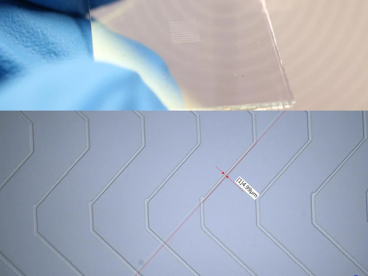
µm-Scale ITO Patterning
Laser-written line structures are demonstrated on an ITO thin film, showing controlled micron-class linewidth and repeatable routing geometry.

Laser Thin-Film & Photonic Processing
薄膜圖案化與光子結構
Precision laser patterning for conductive films, metal layers, liquid-crystal photonic elements, periodic structures and optical waveguide features.
博隆依薄膜與基材堆疊、圖案尺寸、選擇性移除需求及光學功能,規劃雷射波長、偏振、光束形式、掃描路徑、干涉條件與製程 DOE。
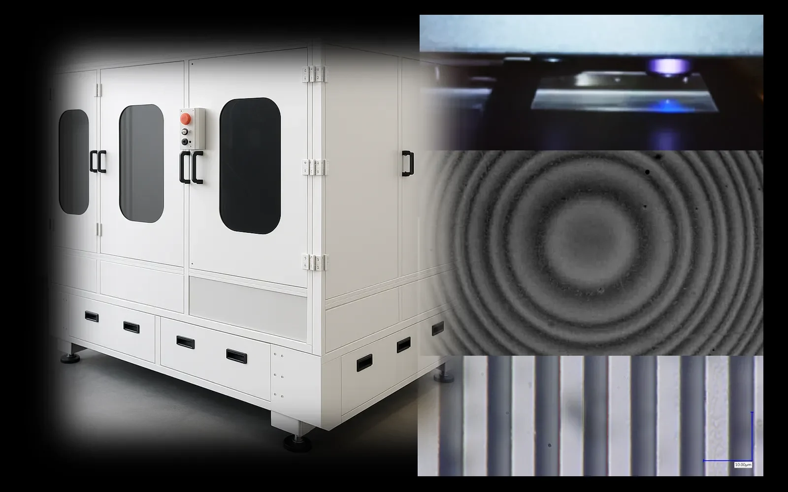
Capability Overview
Bolite develops laser processes for selective thin-film removal, micron-scale circuit definition and photonic-structure formation. The platform supports conductive-film patterning, 3D routing, polarization-controlled photoalignment, laser interference lithography and localized optical-feature fabrication.
博隆會依薄膜吸收特性、基材耐受度、膜厚、線寬/間距、殘留膜要求與功能驗證方式,建立適合的能量密度、焦點、偏振、光束重疊、掃描速度及多道次加工策略。
Key Capabilities
博隆可依透明導電膜、金屬薄膜、液晶光學與光波導元件需求,提供製程可行性評估、DOE、樣品製作、形貌量測及功能驗證規劃。
Demonstrated Results
以下案例展示 ITO 微米級圖案、導電與金屬薄膜選擇性移除、三維微電路路由、液晶幾何相位元件、雷射干涉微影及光波導 45° 反射面。實際規格須依材料堆疊與功能測試確認。
Laser-written line structures are demonstrated on an ITO thin film, showing controlled micron-class linewidth and repeatable routing geometry.
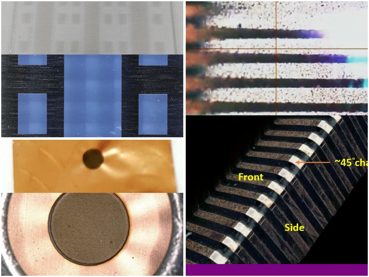
Demonstrated cases include conductive-film opening, localized copper-foil removal and metal-film patterning across a chamfered three-dimensional component.
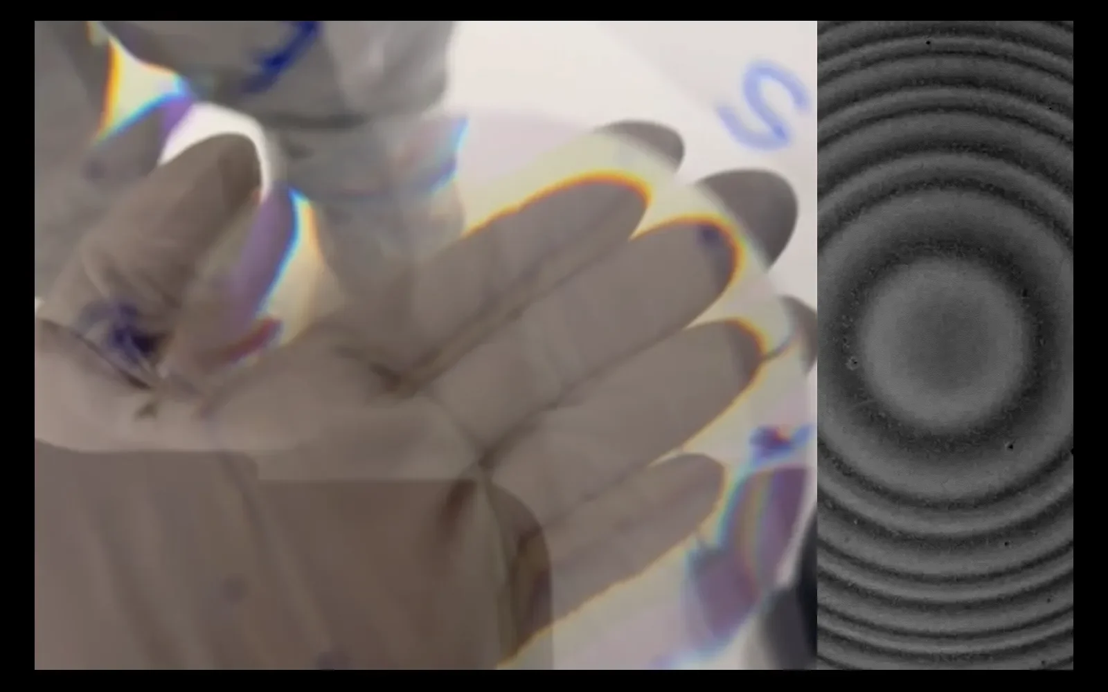
Laser polarization-induced photoalignment enables pixel-by-pixel orientation control for geometric-phase liquid-crystal lens structures.
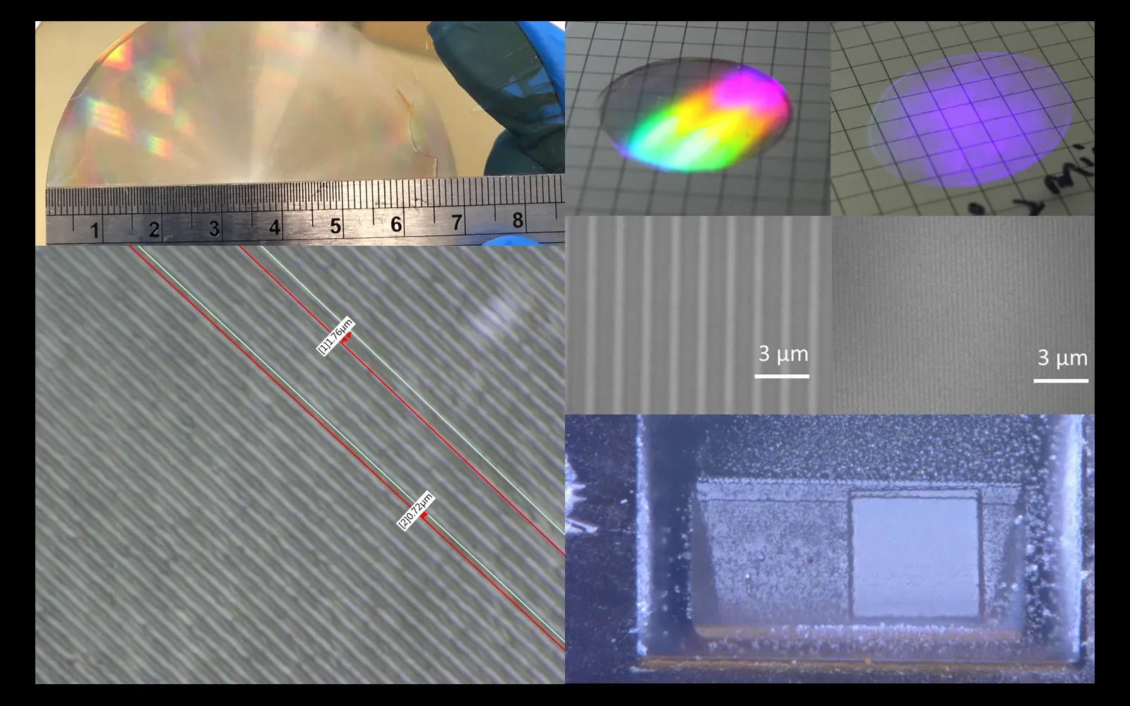
Laser interference lithography creates diverse periodic microstructures, while localized processing demonstrates a 45-degree mirror surface for optical waveguide coupling.
Materials & Structures
實際選擇性、最小線寬、加工邊緣、殘留膜、基材損傷與光學功能,須依膜層成分、厚度、基材、表面狀況與後續量測方式進行評估。
Applications
ITO 電極、感測線路、透明導電圖案與顯示元件製程開發。
液晶取向、幾何相位元件、薄型光學與可程式化偏振結構。
三維零件表面的金屬膜圖案、互連路徑及選擇性絕緣區製作。
光波導反射面、耦光界面、週期性結構及光子封裝原型。
Development Workflow
Information Required
請提供材料堆疊、圖案尺寸、目標加工層、功能需求與驗收方式,博隆可據此規劃雷射選擇、DOE、量測及樣品製作方案。
Minimum feature size, film selectivity, electrical performance and optical efficiency must be verified using the customer's actual material stack, geometry and acceptance method.
Start a Patterning Evaluation
提供薄膜與基材堆疊、圖案檔、線寬/間距、加工區域、電性或光學驗收要求,博隆技術團隊將協助評估雷射圖案化與功能結構製程。詳細參數與專有技術可於 NDA 與專案協議下進一步討論。